
Goal:
You will understand some of the basic principles of designing with an op-amp, including its use in buffering, balanced/unbalanced audio and amplification.
NOTE: This is a component that requires a dual power supply. Connecting this incorrectly can DAMAGE the op-amp. Please be careful. You will pay for any op-amp you damage ($7 for the OPA2134). These devices get warm in operation but if they are hot to the touch then you have probably wired something wrong and should immediately depower the circuit!
Passive Mixer Issues
In the passive mixer lab 4 major issues were encountered.
1. It was not possible to amplify signals.
Because there was no power supply we couldn’t turn the signal up, so the passive mixer requires already amplified signals and the passive mixer can only turn signals down.
2. Everytime an input is pulled out or plugged in the impedance of the circuit changes (There was no buffer). We didn’t focus on this specifically.
This often doesn’t matter if all we care about is basic splits or only passive features.
3. Separating signals and assigning them to other buses was not possible without mixing the buses.
Meaning if you wanted inputs 1 and 2 to go to output 1 that was fine, you would make a bus to do so, but if you also wanted just output 1 to go to output 2 now you have an issue because 1 is connected to a bus. There is no purely passive way to have both connections at the same time.
4. Controlling the gain of specific signals on a bus was not possible.
Moving a volume control would affect all other signals on the bus as well.
The Op-Amp can solve all of these issues and with the op-amp we will enter the world of active mixing.
Active Mixing
An active mixer uses a power supply to do its job. That is all active means. Active mixers are the most flexible hence why you see them everywhere. They solve all the issues talked about in the passive-mixer section, a key component in these designs is the op-amp.
The Op-Amp
The op-amp’s full name is the operational amplifier. These little guys are capable of doing many jobs. They can carry out math functions, act as a comparator, and of course act as an amplifier. The inner workings of an op-amp are very complex. It boils down to many transistors in various amplifier topologies to form one “big” amplifier. There are many op-amps out there, some are more expensive than others and they all have different spec’s determined by their internals but at the end of the day they do those 3 jobs with different degrees of performance.
- Execute Operations on a signal (Math)
- Amplify Signal
- Compare Inputs
We will treat the op-amp as a “black box” or in other words we won’t worry about how the insides work. Just like how you can learn to drive without knowing how to build a car or how its inner mechanics work, you can learn to design with an op-amp without knowing its internals. There are many cars with different performance characteristics and those things may matter to you but you simply don’t need to know all the details of the car to use it. Op-amps are like that.
The schematic Symbol for an op-amp is a triangle:

There are 5 terminals we must satisfy for it to work. First is the power, pins 5 and 4. There is a positive power supply and a negative power supply. We need these so that it can amplify the positive part of the wave and the negative part of the wave. There are op-amps that use a single power supply but these cases are beyond this lab currently. The power supply required will be given by the op-amps spec sheet (or data sheet) which can be googled and easily found provided by the manufacturer. These can also be found from the suppliers page where you order the part, if the seller is reputable that is.
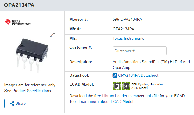
We will be using the OPA2134 op-amp by Texas Instruments their spec sheet says:

Spec sheets can be overwhelming at first but on the first page we see some very useful features listed, namely we see it can handle a voltage range of plus or minus 2.5V to plus or minus 18V! This is great as our 9 volt batteries are in this range. We also note that just above it we see the total distortion is also very low which will be very good for music.
Selecting Power Supply Range
When amplifying a signal the op-amp will use the power provided to it to create the amplified output wave. The power being greater than the peak to peak voltage signal we send in is why amplification is possible. If the power supply is only ±3V then the biggest wave it can produce is close to ±3V since that is our power supply, often called the power rails. Most op-amps can not go all the way to the power rails but some special op-amps called rail to rail op-amps can (and these are more expensive). In general we just need to make sure the op-amp can use the supply we intend to use and also produce the output we need. Rail to rail op-amps are more expensive so it's usually cheaper and easier to just use a higher power supply range than we need to amplify that the op-amp can still comfortably handle. For example, we will use ±9V which is way beyond the amplification we will need so the op-amp should not struggle with voltage.
We could also look at a specific pair of headphones to determine the requirements of the circuit such as the audio-technica M50’s. Their specification on their website gives the following:

To determine the voltage and current required to drive the headphones we must know their impedance. Here we have it as
First we know the power is
So we see that we need 5.1mA and .195 Volts to obtain 99dBSPL. This is very loud and within the specs of most op-amps. Most op-amps can supply up to 10mA. This is a very low impedance load so it will require more current and less voltage compared to a higher impedance pair of headphones. For example a 300 ohm impedance yields 1.8mA and .548V.
Let’s say you want to go up to 110dBSPL. For this we need a way to determine how much more power we need based on how much louder we want to get. We will skip the derivations as it is beyond the scope of this lab and will simply jump right to an equation that can relate how much louder we want to get to the power required. Note that since the dBSPL given was used with a mW reference the answer will also be in mW.
The cheaper TL072 can only provide up to 10mA (this is a common limit with many op-amps) so it will not be able to produce such volumes, but the OPA2134 in the spec sheet says it can output a whopping ±35ma. The TL072 is far cheaper than the OPA2134, but now you can see one reason why the OPA2134 may be selected over the TL072 (and the TL072 is a very old chip 1978 vs the OPA2134 which was created in 1997 according the spec sheet dates from TI). Being old isn’t bad but comparing the spec sheets the OPA2134 has some obvious improvements. There are several other cheaper op-amps you could use, the NE5532 being another.
Another cheap and much more standard solution to the current demand issue is to use transistors, specifically a class B amplifier but this gets much more complex so we will use a simpler less capable circuit for now. Just know that if it doesn’t sound so great it's probably because your impedance is so low causing that its a current demand to high for the op-amp.
Headphone Impedance
A quick note about the impedance of headphones, impedance does not directly tell you about the “quality” of headphones. One common point of higher impedance headphones is the fact that the driver in the headphones now requires a great voltage change to change the physical movement of the driver leading to “finer” control. Other design factors, such as acoustic focused ones, however often overshadow this making impedance not a good consideration for the “quality” of the headphones. This is one reason “hi-fi” headphones are often higher impedance (above 100 ohms is a common cutt-off for high impedance vs low impedance though no standard rule exists). Instead it should only really be alarming if it is very high or low. If it's too low you run into current demand issues and too high runs into voltage demand issues. We are looking for a balance. Most consumer devices expect to drive things below 100 ohms and many studio devices expect things above 100 ohms. High impedance headphones will struggle to get very loud with many consumer device outputs. It boils down to use case over “quality” in most cases. I recommend getting something between 30 and 100 ohms.
DIPS
DIP’s (Dual inline packaging) or “chips” often have many op-amps in a single chip, hence a TL071 has 1 op-amp in a chip, while a TL072 has 2 and a TL074 has 4. They look like this:

The front of the chip is shown by the little dot or an indent, this defines where pin one is. Pins are always counted this way. Here we have the layout of the OPA2134:

This pin-out for dual op-amp packages is very common so it can be easily swapped with other dual op-amp chips, such as the NE5532. However, always make sure to check the chip pin-outs to ensure this is this case! This also holds true for many quad op-amp chips as well.
Writing these types of chips on a schematic is a little different, here we have 2 op-amps, so 2 triangles will be needed. The convention I’ve always seen is if there is more than one chip then they are numbered, while the internal op-amps are lettered. So we would have chip 1 op-amp A, chip 1 op-amp B ect. Usually the power supply pins are also given a letter, in this case it's chip 1 unit C which are really the power pins.

Here KiCad has not yet numbered the chips so it has a “?” instead of a number. It is common practice to move the power pins off to the side to make reading the schematic easier, we see pin 8 would go to V+ and pin 4 would go to V- exactly as the pin out says. It is important you understand how the pin-outs on the schematic relate to the physical chip or else you won’t be able to build it!
The 3 Op-Amp Rules
Note that these rules are idealized but will be fine assumptions for this class.
- No current passes through the input terminals.
- The potential difference between the inputs is 0.
- Open loop gain is infinite.
Rule 1
Rule 1 means that if there is a connection to pin 1 and pin 2 no current would flow from pin 1 to pin 2. This becomes important in feedback circuits.
-Source:
In this configuration current will flow from Vin through R1, when it reaches the inverting input (Pin 2 on the symbol with the “-” sign) the current will not be able to flow to the non-inverting input (pin 3 with the “+” sign) because of the op-amp rule (in reality there is an incredibly high impedance there), therefore the current will flow up to R2 and down to Vout.
Rule 2
The potential difference between inputs simply means the voltage at the inverting input is the same as the voltage at the non-inverting input, or in other words pin 1 and pin 2 have the same voltage.
In the example above we see the non-inverting input is tied to ground which is 0 Volts, this means the inverting inputs pin must have 0 volts as well.
Rule 3
The open loop gain being infinite means when no feedback is connected, meaning the output does not tie back to one of the inputs, then the gain of the op-amp will be infinite. Obviously in reality this is not true but it is an incredibly large number, anywhere from 20K to 100K. This gain is so high it's not useful for music. Therefore we use feedback to get control over the value of the gain so it can be usable.
Experiment 1 The Buffer
One of the most useful and simple configurations of an op-amp is as a buffer. The op-amp has the ability to ensure what comes in is what goes out, meaning the impedance no longer changes when plugging in headphones or taking them out!
Consider the following:

Here a signal is connected to the non-inverting input. However, it is not connected to anything else. Using the golden op-amp rules we know the voltage on 3 must match the voltage on 2.
Therefore pin 2 now gets the signal and transfers that to the output.
This may seem trivial but the op-amp provides a very high input impedance and a very low output impedance. These are desirable because now even with very small ohmage loads they will still be driven and not load the circuit. With buffers we can have many small ohm loads and large ohm loads and it will not impact the performance of other outputs.
Because this circuit copies the input to the output or in other words it “follows” the voltage it is often called a voltage follower.
Build The Following

Reading the schematic:
Here is the first schematic that uses nodes. Circuit schematics can look much neater by using a node. Here we have 3 such nodes. A ground node, and V+ node and a V- node. Each node is a short hand so that parts of the circuit on the schematic don’t need lines everywhere. They are still connected via wires in real life but on the schematic it is understood these points are connected because they have the same node name.
When wiring up a DIP (the op-amp in our case) be sure to have the pin layout from the data sheet! This one:
Schematics should have the pin number on them but it is always a good idea to double check the pin numbers on the schematic match the spec sheet. In this case we see Vcc- and Vcc+ are pins 4 and 8 which agree with the spec sheet (the picture above). The ground node shown is a circuit ground for our understanding. All parts of the circuit with this node should be connected via a wire. For ground I usually make a rail on the breadboard the “ground” rail. If we want to measure the voltage of a part of the circuit then our reference 0V point (where we put the black lead) will be that node.
Stability
The 100k resistors are very important for increased stability. They may not be strictly needed but there will be times with some op-amps where an awful noise will happen if you don’t have these! They prevent 2 major issues, the first is a floating pin. Assume the resistors are not present and there is no tie to ground. When no input is connected the input pins on the op-amp are said to be floating. This just means that the signal has no tie to a voltage reference in the circuit, making it susceptible to interference. In this condition some op-amps may start oscillating like crazy (which will be very loud, unpleasant and unwanted). To fix this we place a large resistance tying the input to ground this way when no input is connected the path through the resistor will still provide a path to ground. This stops issue 1. (Has happened with the NE5532 in my experience, I’ve yet to have a TL072 or OPA2134 do this but it's still a good idea.)
Issue 2 is clicking and popping when plugging something in or pulling something out. If there were no resistor to ground again the pin would be floating and this means when something is plugged it suddenly has a reference to the circuit's ground and will “pop” or adjust to that reference. To prevent this issue we can just provide a reference to it, this way when something is plugged in no adjustment will be needed.
We want this resistance to be very high to prevent interfering with the circuit's operation when something is plugged in.
Interpreting the circuit:
This circuit is the same as an aux cable but now both channels are buffered. You should be able to hear your music clearly given your current demand is not too much.
The power supply might seem unusual at first. Each battery is worth 9 volts. Going from the negative side to the positive side we rise by 9 volts. That's how a battery works right? Now is where defining circuit ground will matter. Remember, we can pick where we place 0. It is similar to how we may be on the 2nd floor of a 4 floor building but we decide to call it ground anyways. In that situation the floor beneath us becomes floor -1 and the floor we are on is floor 0, the floors above now become floor 2 and 3. We just gave them new names. We could call the floor connected directly to the earth “ground”, and in that case the bottom floor or “earth ground” is floor 0, the next floor up is floor 1, the floor above that is floor 2 ect… It’s a matter of perspective.
Here we have 2 batteries in series. We take the middle to be ground (0 volts), which is our “perspective”. Therefore going from ground in either direction will have us change by 9 volts. If 0V is in the middle then going up we go from 0 volts to 9 volts, therefore the top is 9 volts. However from the middle when we go down we go from 0V down 9 volts therefore the bottom is now -9 volts.
When a power supply is done this way it is said to be floating. This is because the spot we are calling 0 volts is not an absolute reference. Earth ground for example would be such a reference. Just like in our analogy of the floor of a building calling the 1 floor above the ground “floor 0” is not truly “on the ground”, instead it's a “floating ground”. The circuit could be viewed differently for example if the ground was moved to the bottom of the batteries like so:

This would put the V- at 0 volts and V+ at 18 volts since we now rise over 2 batteries relative to circuit ground. We don’t use this configuration however because now there is no room for the negative part of the wave! If we were to connect the OPA2134 to this it would only have room to go up. It is like how if we are on the ground floor we cannot go any lower! (assuming there are no basement floors) BUT if we start on floor 1 and call that “ground” then we have room to go both up and down which is exactly what an AC voltage will want to do!
Questions
- What are the benefits of a buffer?
- What are the three golden rules of op-amps?
- What does it mean for a ground to be “floating”?
- For a pair of headphones with a sensitivity rating of 100 dB and an impedance of 100 ohms what is the voltage and current demands. Show your work.
Lab Design Questions
Must be done in class!
Submit a picture of each working (lights are on) design on the breadboard. You could include off and on states if you want to be fancy. Be sure to include the current limiting resistor we talked about before or you will burn out the led! You may work in groups.
- In the schematic above add volume controls by using potentiometers (wired the same way the passive mixer lab explains).
- (CHALLENGE DESIGN, OPTIONAL) Create a schematic in which 4 inputs are delivered to 4 outputs using TS jacks (AudioJack2 in Kicad). Each input should have its own volume control be buffered, go to a bus and each output should be buffered.
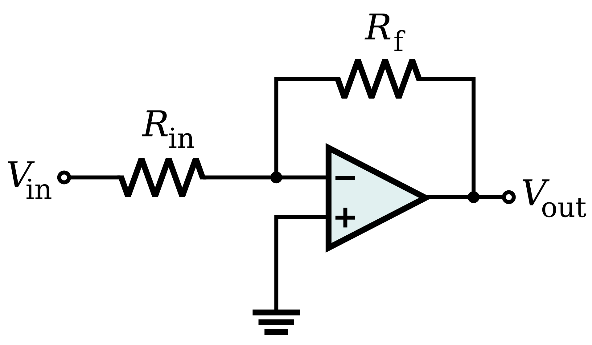
Experiment 2 The Inverting Amplifier
The inverting amplifier is the first amplifier we will look at that can control the volume. It is configured like so:

When the output is connected to the inverting input it is called negative feedback. When the output is connected to the non-inverting input it is called positive feedback. Here we have a case of negative feedback. The Rout resistor is sometimes called Rf for feedback since that is the path the feedback happens through.
We can derive the gain of this circuit using the properties of op-amps, the voltage law and current law. For this class we will skip to the result and learn how to use that. The gain of this circuit is:

The negative sign indicates the voltage will be flipped, or in other words this amplifier will flip the polarity of the wave. If we choose Rf to be the same as Rin then we will have a unity gain amplifier, meaning an amplifier with a gain of 1. If we choose Rin to be large compared to Rf then it will reduce the voltage and if we choose Rin to be small compared to Rf then it will increase the voltage.
IMPORTANT! If Rin becomes 0 we run into major problems. We will get infinite gain! This makes varying Rin problematic. Such gain could damage parts. For this reason we choose to set Rin to a fixed value so that this cannot happen and instead vary Rf. If Rf becomes 0 then we get 0 as the gain.
Questions
- If Rf is 10K ohm and Rin is 1K ohm what will be the gain?
- If Rf is 500 ohm and Rin is 20k ohm what will be the gain?
- If Rin is zero ohm and Rf is 1 ohm what will be the gain?
If the gain is too high we will clip the output and wind up with all kinds of issues. Therefore, we must keep gain factors reasonable. If we know the input signal range and the range our output expects we can create the gain factor we will need. We saw earlier the computations for a pair of headphones that increased the gain by 11dBSPL. You could use that as a template to determine the gain factor you want. For very small mic signals we will need large gain factors, but for signals that are already amplified less gain will be required.
What we will do is set up a potentiometer to act like a variable resistor. If we make this Rf then we obtain a volume control, or gain control. By setting Rin to a set value we prevent the possibility of infinite gain if we set the volume to low.
Questions 2
- We will use 10K pots. If we desire the max gain to be 10 times the input what must be the value of Rin?
- What if we desire the max gain to be 5 times? 20 times?
For our design lets use a gain factor of 10 as the max. This will yield the following circuit:
Build the following:

Reading the Schematic
Here we have a ground node that appears in multiple places. These should be connected together.
Interpreting the Schematic
We have a pot on each channel. We have a 1k resistor into a 10k pot. This yields a max gain of 10 times the input. This is then passed out. Remember since this is an inverting amplifier the output will be flipped! (Represented by a negative sign on the gain.)
Note that in these circuits the op-amps still work as buffers; the difference is these buffers do not have a fixed gain of 1.
Loading
There is one other issue that can come up. In such a schematic you can run into loading. Loading occurs when the resistance of our source or load becomes significant in the circuit. For example, we are plugging in phones as the input, phones are not ideal voltage sources because they have some amount of resistance. If this resistance is very large then we can run into a problem because that resistance (often called the source resistance because it comes from the voltage source) will be in series with the 1k resistor. This 1k resistor is a key part in what determines our gain but if that number is increased by the source then our gain will be very different!
We use the term input impedance to talk about the amount of resistance the input of the circuit sees when no input is present. (We won’t worry about how to find the input impedance, I just want you to understand what loading is.) In our circuit it is 1k. We designed our circuit to run like this and we assumed that the source would not add any additional impedance. If however our input has a resistance of 500 ohms then the real value of the equivalent R1 is 1500 ohms! This will change the gain a lot!
For this reason we want the source impedance to be as small as possible. We could also solve the problem by making the input impedance (R1) very large compared to the source resistance so that it doesn’t matter. Generally at least a factor of 10 is enough. Another way to solve this issue is to add a buffer stage which will make it so the impedance of the source has no real impact on the circuit, we could plug-in just about anything (assuming the op-amp can handle the current and voltage demands). A similar issue happens on the output of the circuit, and this is why buffers are so useful. Op-amp buffers offer us very high input resistance (so that input source resistance doesn’t matter much) and very low output resistance (so that the load “sees” only the resistance that it has and not any resistance the circuit may have left).
At the end of the day just know a buffer may be needed to prevent loading. This is a very good idea if you don’t know the type of circuit you will be dealing with and have a poor input or output impedance for your application.
Note: When our input went right to the op-amp this was not an issue because the op-amp has a very large input resistance.
Questions
- What will happen if instead of wiring pins 1 and 2 together I wire pins 3 and 2 together on the potentiometers?
Lab Design Questions
- Create a schematic that uses only inverting amplifiers but whose output is not flipped.
Experiment 3 The Non-Inverting Amplifier
There are configurations which yield an output that is not inverted and still give us gain control. Here such a configuration:

Here the input is fed into the non-inverting input while the inverting input is grounded through a resistor. Again the gain equation can be found using the basic op-amp rules and circuit laws but we will skip to the result:

Note that this circuit contains a constant. This means that if we make Rf=0 (short circuit) and Rin very large (just leave Rin off, we think of it as an “open” which is the closest we have to infinite resistance) then we get a constant gain of 1. This is exactly the same circuit as the unity buffer circuit!
The non-inverting amplifier circuit cannot go below a gain of 1 so there is no way to reduce the voltage and by extension the volume. As a result we may instead wish to build an inverting stage if we desire volume control that can get softer as well as louder.
If we wish to implement this on a stereo output the circuit would be as follows:
Build the following:

Once again we have a potentiometer to act as a variable resistor just like the previous amplifier.
Questions
- Is this circuit a 1 channel or 2 channel circuit?
- What is the gain of this circuit if the pot is at 10k ohm and Rin is as shown on the schematic?
- What type of feedback is this circuit using?
Experiment 4 The Summing Amplifier
Up to now we have only built circuits that deal with 2 channels, but mixing may have many channels. In passive mixing once sounds are on a bus they share a volume control, meaning you can’t selectively turn down 1 channel in a bus that has 3 channels on it, all 3 will be affected by the pot. However an active mixer can do this.
This is where the summing mixer comes into play.

This looks just like the inverting amp only now we have multiple inputs reaching a common node called the summing node. Again we will take the gain equation for granted.

Importantly note that since this is an expanded inverting amplifier the polarity is flipped! If we listen to it this will be just fine (our ears don’t detect things like polarity flips) but if we mix this with a signal that has not been flipped we will definitely hear it! Therefore it is a good idea to invert it one more time through a unity inverting amplifier so that the output and input are “in phase”.
The reason this circuit can isolate inputs and sum them is because the summing node, pin 2, is forced to 0V by our op-amp rules. This has the effect of isolating the various inputs.
A Brief Note about Phase and Polarity
I should say here you will see phase used a lot in texts implying a 180° phase shift. This is not what is happening. Instead we have a signal inversion. If it was just a phase shift then things like saw waves would not cancel out but this circuit will flip it or invert the wave so a saw wave that is not inverted (didn't go through the circuit) will cancel out. Phase here is used with the notion of a sine wave because a 180° shift of a sine wave does cancel out with its unshifted version since in the sine wave case such a shift is the same thing as a polarity flip. So we often say things like “the input and the output are out of phase” when in reality it is really a polarity flip.
Loading
This circuit can also suffer from the loading effect as well, making it so that adding a buffer stage before the input can be a good idea for each input. We will not do so in our simple schematic.
Adding Volume Controls
The current circuit simply adds the voltages when we would really like to have control over how much of each input is added. To do this we want control over the voltage input that is driving the circuit. We cannot simply replace Rin with a pot because if that goes to 0 we will get infinite gain which is bad. Therefore instead we add a pot as a voltage divider that directly controls how much voltage is sent into the circuit. This way we can leave Rin fixed avoiding the issue of infinite gain.
We also change Rf for a pot like before to act as a master gain for the entire summing circuit just like we did in the inverting amplifier section.
The final circuit will look like this:

Here I adjusted this circuit so that it only uses 2 inputs and 2 outputs but in theory you can add more.
Now we have control over the volume of 2 inputs that sum down to one bus to be delivered to the output.
Questions
- Add a buffer to each input, submit your answer as a schematic.
- Add an inverting amplifier output stage, submit your answer as a schematic (you do not need to keep the buffers from question 1 in the circuit).
- With the inverting amplifier output stage from question 2 are the inputs and outputs “in phase” or “out of phase”?
Adding Busses
Now that we have created a summing mixer you may want to group channels. In our simple 2 in 2 out example above both outputs had both inputs. What if we instead wanted output 2 to have both inputs but output 1 to only have input 1?
In this situation we can simply tap an output before the summing circuit. If we do it right after the pot then the pot will still act as a volume control, if we do it before the pot then the pot’s movement will have no effect on the volume of that output, just like a pre-fader switch! We will take the output from before the pot. We again can run into issues with impedances, therefore we will add a buffer on this line.
Build the following:

Much more complex systems can be created via switches to allow for multiple buses with their own dedicated faders.
Design Question
Submit your answer as a schematic.
- Create a schematic that adds a gain control to output 1 (the top output).
Experiment 5 The Differential Amplifier (Balanced Audio)
Balanced and unbalanced audio is very handy. When audio travels through a wire it can obtain additional noise. This noise is seen on the output and is undesirable. To fix this we can use a balanced connection. This is a connection where the same signal is sent down 2 channelsbut on one of the channels the signal isinverted.
As the signal travels down the cable both channels will pick up the same noise. Once the cable reaches its destination one of the signals will be flipped so the signals are constructively interfering meaning they will sum and the noise is deconstructively interferingmeaning it will cancel out!A connection that does this is said to be balanced. A connection that does not do this is said to be unbalanced.
This is why TS connectors are always unbalanced. They don’t have the extra channel required! TRS connections can be balanced or unbalanced. If the TRS cable is plugged into a balanced output (one that has the 2 channels being output but one is inverted) then it will carry a balanced signal and is said to be balanced mono. Or it can carry two unique channels such as left and right audio and is said to be unbalanced stereo.If you want balanced stereo you would need 5 connectors, one for both left and right, their flipped signals, and a ground connector. Such a connector would be a TRRRS. Note, there is no such thing as a balanced “cable” it is about what you plug the cable into! Sometimes you will hear cables referred to this way and it can lead to confusion.
Since TRS can be both balanced and unbalanced depending on what your input and output says there is another standard, the XLR. XLR cables are understood to always be used with balanced inputs and outputs.
Such flipping can easily be achieved with inverting amplifiers and the tools we already discussed.
Say we are designing a device that expects a balanced input. This means the cable that is plugged in will have a channel that is flipped and a channel that is not flipped. We need to unflip the flipped one so the noise will cancel out and we can use the signal on the cable, otherwise the signal will cancel itself out and we will be left with noise! The ring is the standard channel to be flipped.
So we must create an input that will flip the ring channel, then sum them together to create 1 channel of audio. All we need is an inverting amp and summing amp:

It is optional to build this one but if you ever plan to work with balanced signals you should be very capable of handling the inputs and outputs!
Questions
- Design a circuit that takes an unbalanced signal (assume is the same signal on both ring and tip) and creates a balanced output. Submit your answer as a schematic.
- (OPTIONAL CHALLENGE QUESTION) Design a schematic that takes a balanced stereo in and outputs unbalanced stereo.
Final Questions
- What causes a circuit to be loaded?
- What would happen if you plugged an unbalanced stereo TRS into a balanced input?
- Why would one choose to use a balanced connection over an unbalanced connection?
CMoy Headphone Amp
Build the following circuit and submit a picture of the breadboard in your report.

The “u” stands for the greek letter μ so C1 is .1 microFarads (10-6 is micro). The potentiometer here is a dual potentiometer. You could replace this with 2 separate 10k pots. Pins 1 and 4 match as do 2 to 5 and 6 to 3.
The capacitors serve as a filter. If you like you could insert a switch to control power.